

How To Draw A Cmos Circuit

Complementary metal–oxide–semiconductor (CMOS, pronounced "see-moss"), also known equally complementary-symmetry metal–oxide–semiconductor (COS-MOS), is a type of metal–oxide–semiconductor field-issue transistor (MOSFET) fabrication process that uses complementary and symmetrical pairs of p-type and north-type MOSFETs for logic functions.[ane] CMOS technology is used for amalgam integrated circuit (IC) fries, including microprocessors, microcontrollers, retention chips (including CMOS BIOS), and other digital logic circuits. CMOS engineering is as well used for analog circuits such as image sensors (CMOS sensors), information converters, RF circuits (RF CMOS), and highly integrated transceivers for many types of advice.
Mohamed Grand. Atalla and Dawon Kahng invented the MOSFET at Bong Labs in 1959, and and so demonstrated the PMOS (p-type MOS) and NMOS (n-type MOS) fabrication processes in 1960. These processes were later combined and adjusted into the complementary MOS (CMOS) process by Chih-Tang Sah and Frank Wanlass at Fairchild Semiconductor in 1963. RCA commercialized the technology with the trademark "COS-MOS" in the late 1960s, forcing other manufacturers to find some other name, leading to "CMOS" becoming the standard name for the technology by the early 1970s. CMOS eventually overtook NMOS equally the dominant MOSFET fabrication process for very large-scale integration (VLSI) fries in the 1980s, while also replacing earlier transistor–transistor logic (TTL) technology. CMOS has since remained the standard fabrication process for MOSFET semiconductor devices in VLSI chips. Every bit of 2022[update], 99% of IC chips, including almost digital, analog and mixed-bespeak ICs, are fabricated using CMOS applied science.[ii]
Two of import characteristics of CMOS devices are high noise immunity and low static ability consumption.[3] Since 1 transistor of the MOSFET pair is always off, the series combination draws significant power only momentarily during switching between on and off states. Consequently, CMOS devices do not produce equally much waste heat as other forms of logic, like NMOS logic or transistor–transistor logic (TTL), which commonly have some standing current even when not changing state. These characteristics permit CMOS to integrate a high density of logic functions on a chip. It was primarily for this reason that CMOS became the near widely used technology to be implemented in VLSI fries.
The phrase "metal–oxide–semiconductor" is a reference to the physical structure of MOS field-consequence transistors, having a metal gate electrode placed on tiptop of an oxide insulator, which in plough is on top of a semiconductor fabric. Aluminium was one time used simply now the cloth is polysilicon. Other metallic gates have made a improvement with the appearance of high-κ dielectric materials in the CMOS process, equally announced by IBM and Intel for the 45 nanometer node and smaller sizes.[4]
Technical details [edit]
"CMOS" refers to both a particular style of digital circuitry pattern and the family of processes used to implement that circuitry on integrated circuits (chips). CMOS circuitry dissipates less ability than logic families with resistive loads. Since this advantage has increased and grown more important, CMOS processes and variants have come to boss, thus the vast majority of modern integrated circuit manufacturing is on CMOS processes.[5] CMOS logic consumes over 7times less power than NMOS logic,[half dozen] and nearly 100,000 times less power than bipolar transistor-transistor logic (TTL).[7] [8]
CMOS circuits employ a combination of p-type and n-blazon metallic–oxide–semiconductor field-upshot transistor (MOSFETs) to implement logic gates and other digital circuits. Although CMOS logic can be implemented with discrete devices for demonstrations, commercial CMOS products are integrated circuits composed of up to billions of transistors of both types, on a rectangular piece of silicon of betwixt ten and 400 mm2.[ citation needed ]
CMOS e'er uses all enhancement-fashion MOSFETs (in other words, a zero gate-to-source voltage turns the transistor off).[ix]
History [edit]
The principle of complementary symmetry was first introduced by George Sziklai in 1953 who and then discussed several complementary bipolar circuits. Paul Weimer, besides at RCA, invented in 1962 TFT complementary circuits, a close relative of CMOS. He invented complementary flip-flop and inverter circuits, but did no piece of work in a more than circuitous complementary logic. He was the commencement person able to put p-channel and n-channel TFTs in a circuit on the same substrate. Three years earlier, John T. Wallmark and Sanford M. Marcus published a diversity of complex logic functions implemented every bit integrated circuits using JFETs, including complementary memory circuits. Frank Wanlass was familiar with work done by Weimer at RCA.[10] [11] [12] [13] [fourteen] [fifteen]
The MOSFET (metal-oxide-semiconductor field-effect transistor, or MOS transistor) was invented past Mohamed M. Atalla and Dawon Kahng at Bong Labs in 1959. There were originally two types of MOSFET fabrication processes, PMOS (p-type MOS) and NMOS (n-type MOS).[16] Both types were developed by Atalla and Kahng when they originally invented the MOSFET, fabricating both PMOS and NMOS devices with 20 µm and then 10 µm gate lengths in 1960.[17] [18] While the MOSFET was initially overlooked and ignored by Bell Labs in favour of bipolar transistors,[17] the MOSFET invention generated pregnant interest at Fairchild Semiconductor.[16] Based on Atalla's work,[nineteen] Chih-Tang Sah introduced MOS engineering to Fairchild with his MOS-controlled tetrode fabricated in tardily 1960.[16]
A new type of MOSFET logic combining both the PMOS and NMOS processes was developed, chosen complementary MOS (CMOS), past Chih-Tang Sah and Frank Wanlass at Fairchild. In February 1963, they published the invention in a research newspaper.[20] [21] Wanlass after filed Usa patent 3,356,858 for CMOS circuitry in June 1963, and it was granted in 1967. In both the research paper and the patent, the fabrication of CMOS devices was outlined, on the basis of thermal oxidation of a silicon substrate to yield a layer of silicon dioxide located between the drain contact and the source contact.[22] [21]
CMOS was commercialised past RCA in the belatedly 1960s. RCA adopted CMOS for the design of integrated circuits (ICs), developing CMOS circuits for an Air Forcefulness computer in 1965 and so a 288-bit CMOS SRAM memory scrap in 1968.[20] RCA likewise used CMOS for its 4000-series integrated circuits in 1968, starting with a 20μm semiconductor manufacturing process before gradually scaling to a 10 μm procedure over the adjacent several years.[23]
CMOS applied science was initially overlooked past the American semiconductor industry in favour of NMOS, which was more powerful at the time. However, CMOS was rapidly adopted and further advanced past Japanese semiconductor manufacturers due to its low power consumption, leading to the rise of the Japanese semiconductor manufacture.[24] Toshiba developed C²MOS (Clocked CMOS), a circuit technology with lower power consumption and faster operating speed than ordinary CMOS, in 1969. Toshiba used its C²MOS engineering to develop a large-scale integration (LSI) chip for Sharp's Elsi Mini LED pocket computer, adult in 1971 and released in 1972.[25] Suwa Seikosha (at present Seiko Epson) began developing a CMOS IC chip for a Seiko quartz watch in 1969, and began mass-production with the launch of the Seiko Analog Quartz 38SQW picket in 1971.[26] The first mass-produced CMOS consumer electronic product was the Hamilton Pulsar "Wrist Estimator" digital watch, released in 1970.[27] Due to depression power consumption, CMOS logic has been widely used for calculators and watches since the 1970s.[6]
The earliest microprocessors in the early 1970s were PMOS processors, which initially dominated the early microprocessor industry. Past the tardily 1970s, NMOS microprocessors had overtaken PMOS processors.[28] CMOS microprocessors were introduced in 1975, with the Intersil 6100,[28] and RCA CDP 1801.[29] However, CMOS processors did non get dominant until the 1980s.[28]
CMOS was initially slower than NMOS logic, thus NMOS was more than widely used for computers in the 1970s.[6] The Intel 5101 (1kb SRAM) CMOS memory fleck (1974) had an access time of 800ns,[thirty] [31] whereas the fastest NMOS chip at the time, the Intel 2147 (4kb SRAM) HMOS retention chip (1976), had an access time of 55/lxxns.[6] [31] In 1978, a Hitachi research team led by Toshiaki Masuhara introduced the twin-well Hi-CMOS process, with its HM6147 (fourkb SRAM) retentivity fleck, manufactured with a 3 μm process.[6] [32] [33] The Hitachi HM6147 chip was able to match the functioning (55/70ns admission) of the Intel 2147 HMOS bit, while the HM6147 also consumed significantly less power (15mA) than the 2147 (110mA). With comparable operation and much less power consumption, the twin-well CMOS process eventually overtook NMOS equally the most common semiconductor manufacturing process for computers in the 1980s.[half-dozen]
In the 1980s, CMOS microprocessors overtook NMOS microprocessors.[28] NASA's Galileo spacecraft, sent to orbit Jupiter in 1989, used the RCA 1802 CMOS microprocessor due to depression power consumption.[27]
Intel introduced a 1.5 μm process for CMOS semiconductor device fabrication in 1983.[34] In the mid-1980s, Bijan Davari of IBM developed high-functioning, low-voltage, deep sub-micron CMOS engineering science, which enabled the development of faster computers as well equally portable computers and battery-powered handheld electronics.[35] In 1988, Davari led an IBM team that demonstrated a loftier-performance 250 nanometer CMOS process.[36]
Fujitsu commercialized a 700nm CMOS procedure in 1987,[34] and and then Hitachi, Mitsubishi Electric, NEC and Toshiba commercialized 500nm CMOS in 1989.[37] In 1993, Sony commercialized a 350nm CMOS process, while Hitachi and NEC commercialized 250nm CMOS. Hitachi introduced a 160nm CMOS process in 1995, then Mitsubishi introduced 150nm CMOS in 1996, and then Samsung Electronics introduced 140nm in 1999.[37]
In 2000, Gurtej Singh Sandhu and Trung T. Doan at Micron Engineering science invented atomic layer deposition High-κ dielectric films, leading to the development of a toll-constructive 90 nm CMOS procedure.[35] [38] Toshiba and Sony developed a 65 nm CMOS process in 2002,[39] and then TSMC initiated the development of 45 nm CMOS logic in 2004.[twoscore] The development of pitch double patterning by Gurtej Singh Sandhu at Micron Engineering science led to the development of thirtynm class CMOS in the 2000s.[35]
CMOS is used in most modern LSI and VLSI devices.[vi] As of 2022, CPUs with the best functioning per watt each yr have been CMOS static logic since 1976.[ commendation needed ] As of 2022, planar CMOS engineering is all the same the most common form of semiconductor device fabrication, but is gradually existence replaced past non-planar FinFET technology, which is capable of manufacturing semiconductor nodes smaller than 20nm.[41]
Inversion [edit]
CMOS circuits are constructed in such a way that all P-type metal–oxide–semiconductor (PMOS) transistors must take either an input from the voltage source or from another PMOS transistor. Similarly, all NMOS transistors must accept either an input from ground or from another NMOS transistor. The composition of a PMOS transistor creates low resistance between its source and drain contacts when a low gate voltage is applied and high resistance when a high gate voltage is applied. On the other mitt, the composition of an NMOS transistor creates high resistance between source and drain when a low gate voltage is applied and low resistance when a high gate voltage is applied. CMOS accomplishes electric current reduction past complementing every nMOSFET with a pMOSFET and connecting both gates and both drains together. A high voltage on the gates volition cause the nMOSFET to carry and the pMOSFET non to acquit, while a low voltage on the gates causes the reverse. This arrangement greatly reduces power consumption and estrus generation. However, during the switching fourth dimension, both MOSFETs conduct briefly equally the gate voltage goes from one state to another. This induces a brief spike in power consumption and becomes a serious issue at high frequencies.

Static CMOS inverter. Vdd and Vss are continuing for bleed and source respectively.
The side by side epitome shows what happens when an input is connected to both a PMOS transistor (tiptop of diagram) and an NMOS transistor (lesser of diagram). Vdd is some positive voltage connected to a power supply and Vss is ground. A is the input and Q is the output.
When the voltage of A is low (i.eastward. shut to Vss), the NMOS transistor's channel is in a high resistance country, disconnecting Vss from Q. The PMOS transistor's channel is in a low resistance state, connecting Vdd to Q. Q, therefore, registers Vdd.
On the other hand, when the voltage of A is high (i.due east. close to Vdd), the PMOS transistor is in a high resistance state, disconnecting Vdd from Q. The NMOS transistor is in a low resistance state, connecting Vss to Q. Now, Q registers Vss.
In short, the outputs of the PMOS and NMOS transistors are complementary such that when the input is low, the output is high, and when the input is high, the output is low. No matter what the input is, the output is never left floating. Because of this behavior of input and output, the CMOS circuit'due south output is the inverse of the input.
The transistors' resistances are never exactly equal to zero or infinity, and so Q will never exactly equal Vss or Vdd, but Q will always be closer to Vss than A was to Vdd (or vice versa if A were close to Vss). Without this amplification, there would exist a very depression limit to the number of logic gates that could be chained together in serial, and CMOS logic with billions of transistors would be impossible.
Power supply pins [edit]
The power supply pins for CMOS are called FiveDD and VSS, or 5CC and Ground(GND) depending on the manufacturer. VDD and VSS are carryovers from conventional MOS circuits and correspond the drain and source supplies.[42] These do not utilise directly to CMOS, since both supplies are really source supplies. VCC and Footing are carryovers from TTL logic and that classification has been retained with the introduction of the 54C/74C line of CMOS.
Duality [edit]
An important characteristic of a CMOS circuit is the duality that exists between its PMOS transistors and NMOS transistors. A CMOS circuit is created to allow a path always to be from the output to either the power source or ground. To reach this, the ready of all paths to the voltage source must be the complement of the fix of all paths to ground. This tin can be easily accomplished by defining one in terms of the NOT of the other. Due to the De Morgan's laws based logic, the PMOS transistors in parallel have respective NMOS transistors in series while the PMOS transistors in series accept corresponding NMOS transistors in parallel.
Logic [edit]

More than complex logic functions such as those involving AND and OR gates require manipulating the paths between gates to stand for the logic. When a path consists of 2 transistors in series, both transistors must have depression resistance to the corresponding supply voltage, modelling an AND. When a path consists of two transistors in parallel, either i or both of the transistors must have depression resistance to connect the supply voltage to the output, modelling an OR.
Shown on the right is a circuit diagram of a NAND gate in CMOS logic. If both of the A and B inputs are high, then both the NMOS transistors (lesser half of the diagram) volition conduct, neither of the PMOS transistors (top half) will conduct, and a conductive path volition be established betwixt the output and V ss (ground), bringing the output low. If both of the A and B inputs are low, then neither of the NMOS transistors will conduct, while both of the PMOS transistors will conduct, establishing a conductive path betwixt the output and Five dd (voltage source), bringing the output high. If either of the A or B inputs is low, i of the NMOS transistors will not bear, one of the PMOS transistors will, and a conductive path will exist established between the output and Five dd (voltage source), bringing the output high. As the only configuration of the 2 inputs that results in a depression output is when both are high, this circuit implements a NAND (Not AND) logic gate.
An advantage of CMOS over NMOS logic is that both low-to-high and high-to-low output transitions are fast since the (PMOS) pull-upwards transistors have low resistance when switched on, unlike the load resistors in NMOS logic. In addition, the output signal swings the total voltage between the low and high rails. This strong, more well-nigh symmetric response also makes CMOS more than resistant to noise.
See Logical effort for a method of calculating delay in a CMOS circuit.
Example: NAND gate in physical layout [edit]
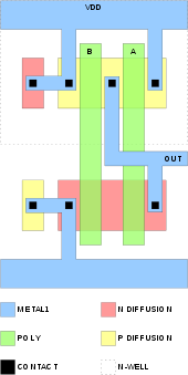
The physical layout of a NAND circuit. The larger regions of N-blazon diffusion and P-type improvidence are part of the transistors. The ii smaller regions on the left are taps to prevent latchup.

Simplified process of fabrication of a CMOS inverter on p-type substrate in semiconductor microfabrication. In step 1, silicon dioxide layers are formed initially through thermal oxidation Annotation: Gate, source and drain contacts are non commonly in the same plane in existent devices, and the diagram is not to calibration.
This example shows a NAND logic device fatigued equally a physical representation equally information technology would be manufactured. The physical layout perspective is a "bird's eye view" of a stack of layers. The circuit is synthetic on a P-type substrate. The polysilicon, diffusion, and northward-well are referred to as "base layers" and are actually inserted into trenches of the P-type substrate. (Come across steps 1 to half dozen in the process diagram below right) The contacts penetrate an insulating layer between the base of operations layers and the offset layer of metal (metal1) making a connection.
The inputs to the NAND (illustrated in green color) are in polysilicon. The transistors (devices) are formed by the intersection of the polysilicon and diffusion; N diffusion for the North device & P diffusion for the P device (illustrated in salmon and yellow coloring respectively). The output ("out") is connected together in metal (illustrated in cyan coloring). Connections between metal and polysilicon or diffusion are made through contacts (illustrated equally black squares). The physical layout example matches the NAND logic circuit given in the previous instance.
The Northward device is manufactured on a P-type substrate while the P device is manufactured in an N-blazon well (northward-well). A P-blazon substrate "tap" is connected to VSS and an North-type n-well tap is continued to VDD to foreclose latchup.

Cantankerous section of two transistors in a CMOS gate, in an N-well CMOS process
Power: switching and leakage [edit]
CMOS logic dissipates less power than NMOS logic circuits because CMOS dissipates power only when switching ("dynamic power"). On a typical ASIC in a modern xc nanometer process, switching the output might have 120 picoseconds, and happens once every 10 nanoseconds. NMOS logic dissipates power whenever the transistor is on, because there is a current path from Vdd to Vss through the load resistor and the northward-type network.
Static CMOS gates are very power efficient because they misemploy nearly aught power when idle. Earlier, the power consumption of CMOS devices was not the major concern while designing fries. Factors similar speed and area dominated the design parameters. As the CMOS applied science moved below sub-micron levels the power consumption per unit area of the fleck has risen tremendously.
Broadly classifying, power dissipation in CMOS circuits occurs because of two components, static and dynamic:
Static dissipation [edit]
Both NMOS and PMOS transistors have a gate–source threshold voltage, below which the current (called sub threshold current) through the device drops exponentially. Historically, CMOS designs operated at supply voltages much larger than their threshold voltages (5dd might have been five V, and Vth for both NMOS and PMOS might have been 700 mV). A special type of the transistor used in some CMOS circuits is the native transistor, with near zilch threshold voltage.
SiO2 is a good insulator, but at very pocket-sized thickness levels electrons can tunnel across the very thin insulation; the probability drops off exponentially with oxide thickness. Tunnelling electric current becomes very important for transistors below 130 nm engineering science with gate oxides of 20 Å or thinner.
Modest reverse leakage currents are formed due to formation of reverse bias between diffusion regions and wells (for e.g., p-type diffusion vs. n-well), wells and substrate (for east.g., north-well vs. p-substrate). In modernistic procedure diode leakage is very small compared to sub threshold and tunnelling currents, then these may be neglected during power calculations.
If the ratios do not match, and then there might be different currents of PMOS and NMOS; this may lead to imbalance and thus improper current causes the CMOS to oestrus up and dissipate power unnecessarily. Furthermore, recent studies accept shown that leakage power reduces due to aging effects as a trade-off for devices to become slower. [43]
To speed upwardly designs, manufacturers take switched to constructions that have lower voltage thresholds just because of this a modern NMOS transistor with a Fiveth of 200 mV has a pregnant subthreshold leakage current. Designs (e.thousand. desktop processors) which include vast numbers of circuits which are non actively switching yet eat power because of this leakage current. Leakage power is a significant portion of the total power consumed past such designs. Multi-threshold CMOS (MTCMOS), now bachelor from foundries, is one approach to managing leakage power. With MTCMOS, loftier 5th transistors are used when switching speed is non critical, while depression Vth transistors are used in speed sensitive paths. Further technology advances that use even thinner gate dielectrics have an boosted leakage component considering of current tunnelling through the extremely sparse gate dielectric. Using high-κ dielectrics instead of silicon dioxide that is the conventional gate dielectric allows like device functioning, only with a thicker gate insulator, thus avoiding this current. Leakage power reduction using new material and arrangement designs is disquisitional to sustaining scaling of CMOS.[44]
Dynamic dissipation [edit]
Charging and discharging of load capacitances [edit]
CMOS circuits dissipate power past charging the various load capacitances (mostly gate and wire capacitance, but also drain and some source capacitances) whenever they are switched. In one consummate bicycle of CMOS logic, current flows from VDD to the load capacitance to accuse it and then flows from the charged load capacitance (CL) to ground during belch. Therefore, in 1 complete charge/discharge cycle, a total of Q=CLVDD is thus transferred from VDD to ground. Multiply by the switching frequency on the load capacitances to go the electric current used, and multiply by the average voltage again to get the feature switching power dissipated by a CMOS device: .

Since most gates do non operate/switch at every clock cycle, they are often accompanied past a factor , called the activeness gene. Now, the dynamic power dissipation may be re-written as .


A clock in a arrangement has an activity cistron α=1, since it rises and falls every cycle. Most information has an activity gene of 0.one.[45] If correct load capacitance is estimated on a node together with its activity gene, the dynamic power dissipation at that node tin exist calculated effectively.
Brusk-circuit ability [edit]
Since at that place is a finite rise/fall time for both pMOS and nMOS, during transition, for case, from off to on, both the transistors will be on for a small menses of fourth dimension in which current will find a path direct from VDD to ground, hence creating a short-excursion current, sometimes called a crowbar current. Brusque-circuit power dissipation increases with the rise and fall time of the transistors.
This class of power consumption became pregnant in the 1990s every bit wires on chip became narrower and the long wires became more resistive. CMOS gates at the cease of those resistive wires see slow input transitions. Careful pattern which avoids weakly driven long skinny wires reduces this effect, but crowbar ability tin can exist a substantial part of dynamic CMOS power.
Input protection [edit]
Parasitic transistors that are inherent in the CMOS structure may be turned on by input signals outside the normal operating range, e.thou. electrostatic discharges or line reflections. The resulting latch-up may damage or destroy the CMOS device. Clamp diodes are included in CMOS circuits to deal with these signals. Manufacturers' data sheets specify the maximum permitted current that may flow through the diodes.
Analog CMOS [edit]
Besides digital applications, CMOS engineering is also used in analog applications. For example, there are CMOS operational amplifier ICs available in the market. Transmission gates may be used as analog multiplexers instead of indicate relays. CMOS applied science is also widely used for RF circuits all the way to microwave frequencies, in mixed-signal (analog+digital) applications.[ citation needed ]
RF CMOS [edit]
RF CMOS refers to RF circuits (radio frequency circuits) which are based on mixed-signal CMOS integrated circuit technology. They are widely used in wireless telecommunication technology. RF CMOS was developed by Asad Abidi while working at UCLA in the tardily 1980s. This changed the style in which RF circuits were designed, leading to the replacement of discrete bipolar transistors with CMOS integrated circuits in radio transceivers.[46] Information technology enabled sophisticated, depression-price and portable finish-user terminals, and gave ascension to small, low-toll, depression-power and portable units for a wide range of wireless advice systems. This enabled "anytime, anywhere" communication and helped bring about the wireless revolution, leading to the rapid growth of the wireless industry.[47]
The baseband processors[48] [49] and radio transceivers in all modern wireless networking devices and mobile phones are mass-produced using RF CMOS devices.[46] RF CMOS circuits are widely used to transmit and receive wireless signals, in a variety of applications, such equally satellite technology (such as GPS), bluetooth, Wi-Fi, nearly-field communication (NFC), mobile networks (such as 3G and 4G), terrestrial broadcast, and automotive radar applications, amongst other uses.[50]
Examples of commercial RF CMOS chips include Intel's DECT cordless phone, and 802.11 (Wi-Fi) chips created past Atheros and other companies.[51] Commercial RF CMOS products are besides used for Bluetooth and Wireless LAN (WLAN) networks.[52] RF CMOS is also used in the radio transceivers for wireless standards such equally GSM, Wi-Fi, and Bluetooth, transceivers for mobile networks such as 3G, and remote units in wireless sensor networks (WSN).[53]
RF CMOS technology is crucial to modernistic wireless communications, including wireless networks and mobile communication devices. One of the companies that commercialized RF CMOS technology was Infineon. Its bulk CMOS RF switches sell over ibillion units annually, reaching a cumulative 5billion units, equally of 2022[update].[54]
Temperature range [edit]
Conventional CMOS devices work over a range of −55 °C to +125 °C.
There were theoretical indications as early as August 2008 that silicon CMOS volition work down to −233 °C (40 K).[55] Operation temperatures near forty Yard take since been achieved using overclocked AMD Phenom Ii processors with a combination of liquid nitrogen and liquid helium cooling.[56]
Silicon Carbide CMOS devices have been tested for a year at 500°C.[57] [58]
Single-electron MOS transistors [edit]
Ultra pocket-size (L = 20 nm, W = 20 nm) MOSFETs achieve the single-electron limit when operated at cryogenic temperature over a range of −269 °C (4 K) to about −258 °C (15 1000). The transistor displays Coulomb occludent due to progressive charging of electrons one by one. The number of electrons bars in the channel is driven by the gate voltage, starting from an occupation of zero electrons, and it can be fix to 1 or many.[59]
See too [edit]
- Active pixel sensor (CMOS sensor)
- Beyond CMOS
- CMOS amplifier
- Electric (software) – used to lay out CMOS circuits
- FEOL (front-end-of-line) – the first function of IC fabrication process
- Gate equivalent – a technology-contained measure out of excursion complexity
- HCMOS – high-speed CMOS 1982
- LVCMOS
- Magic (software) – used to lay out CMOS circuits
- List of MOSFET applications
- sCMOS
- Thermal oxidation
References [edit]
- ^ "What is CMOS Memory?". Wicked Sago. Archived from the original on 26 September 2022. Retrieved three March 2022.
- ^ Voinigescu, Sorin (2013). High-Frequency Integrated Circuits. Cambridge University Press. p. 164. ISBN9780521873024.
- ^ Fairchild. Application Note 77. "CMOS, the Ideal Logic Family" Archived 2022-01-09 at the Wayback Machine. 1983.
- ^ "Intel® Architecture Leads the Microarchitecture Innovation Field". Intel. Archived from the original on 29 June 2022. Retrieved 2 May 2022.
- ^ Baker, R. Jacob (2008). CMOS: circuit design, layout, and simulation (Second ed.). Wiley-IEEE. p. xxix. ISBN978-0-470-22941-5.
- ^ a b c d e f 1000 "1978: Double-well fast CMOS SRAM (Hitachi)" (PDF). Semiconductor History Museum of Japan. Archived from the original (PDF) on 5 July 2022. Retrieved five July 2022.
- ^ Higgins, Richard J. (1983). Electronics with digital and analog integrated circuits . Prentice-Hall. p. 101. ISBN9780132507042.
The dominant difference is power: CMOS gates can consume about 100,000 times less power than their TTL equivalents!
- ^ Stephens, Carlene; Dennis, Maggie (2000). "Engineering Time: Inventing the Electronic Wristwatch" (PDF). The British Journal for the History of Science. Cambridge University Press. 33 (4): 477–497 (485). doi:x.1017/S0007087400004167. ISSN 0007-0874.
- ^ "What is CMOS?". IONOS Digitalguide . Retrieved 2022-01-21 .
- ^ George Clifford, Sziklai (1953). "Symmetrical Properties of Transistors and Their Applications". Proceedings of the IRE. 41 (6): 717–724. doi:ten.1109/JRPROC.1953.274250. S2CID 51639018.
- ^ Lojek, Bo (2007). History of Semiconductor Applied science. Springer. p. 162. ISBN978-3540342588.
- ^ Ahrons, Richard (2012). "Industrial Research in Microcircuitry at RCA: The Early Years, 1953–1963". IEEE Annals of the History of Computing. 12 (ane): sixty–73. doi:10.1109/MAHC.2011.62. S2CID 18912623.
- ^ "Oral History of Thomas (Tom) Stanley" (PDF).
- ^ "IRE News and Radio Notes". Proceedings of the IRE. 42 (6): 1027–1043. 1954. doi:ten.1109/JRPROC.1954.274784.
- ^ Wallmark, J.T.; Marcus, S.Thou. (1959). "Integrated devices using Direct-Coupled Unipolar Transistor Logic". 1959 IEEE International Solid-State Circuits Briefing. Assimilate of Technical Papers. Vol. EC-viii. pp. 58–59. doi:10.1109/ISSCC.1959.1157035.
- ^ a b c "1960: Metal Oxide Semiconductor (MOS) Transistor Demonstrated". The Silicon Engine: A Timeline of Semiconductors in Computers. Computer History Museum. Retrieved August 31, 2022.
- ^ a b Lojek, Bo (2007). History of Semiconductor Engineering. Springer. pp. 321–3. ISBN9783540342588.
- ^ Voinigescu, Sorin (2013). High-Frequency Integrated Circuits. Cambridge University Press. p. 164. ISBN978-0521873024.
- ^ Sah, Chih-Tang (October 1988). "Evolution of the MOS transistor-from conception to VLSI" (PDF). Proceedings of the IEEE. 76 (10): 1280–1326 (1290). Bibcode:1988IEEEP..76.1280S. doi:10.1109/five.16328. ISSN 0018-9219.
Those of united states active in silicon material and device research during 1956–1960 considered this successful effort by the Bell Labs group led past Atalla to stabilize the silicon surface the nearly of import and significant technology accelerate, which blazed the trail that led to silicon integrated circuit technology developments in the second phase and volume production in the 3rd stage.
- ^ a b "1963: Complementary MOS Circuit Configuration is Invented". Estimator History Museum . Retrieved half dozen July 2022.
- ^ a b Sah, Chih-Tang; Wanlass, Frank (1963). Nanowatt logic using field-effect metallic-oxide semiconductor triodes. 1963 IEEE International Solid-Country Circuits Conference. Assimilate of Technical Papers. Vol. VI. pp. 32–33. doi:10.1109/ISSCC.1963.1157450.
- ^ "Low stand up-by power complementary field consequence circuitry" (PDF).
- ^ Lojek, Bo (2007). History of Semiconductor Engineering. Springer. p. 330. ISBN9783540342588.
- ^ Gilder, George (1990). Microcosm: The Quantum Revolution In Economic science And Applied science . Simon and Schuster. pp. 144–5. ISBN9780671705923.
- ^ "1972 to 1973: CMOS LSI circuits for calculators (Sharp and Toshiba)" (PDF). Semiconductor History Museum of Nippon. Archived from the original (PDF) on 2022-07-06. Retrieved 5 July 2022.
- ^ "Early 1970s: Evolution of CMOS LSI circuits for watches" (PDF). Semiconductor History Museum of Nippon. Archived from the original (PDF) on six July 2022. Retrieved 6 July 2022.
- ^ a b "Tortoise of Transistors Wins the Race - CHM Revolution". Calculator History Museum . Retrieved 22 July 2022.
- ^ a b c d Kuhn, Kelin (2018). "CMOS and Beyond CMOS: Scaling Challenges". High Mobility Materials for CMOS Applications. Woodhead Publishing. p. i. ISBN9780081020623.
- ^ "CDP 1800 μP Commercially available" (PDF). Microcomputer Assimilate. 2 (4): one–iii. Oct 1975. Archived from the original (PDF) on 2022-09-23. Retrieved 2019-07-22 .
- ^ "Silicon Gate MOS 2102A". Intel. Retrieved 27 June 2022.
- ^ a b "A chronological list of Intel products. The products are sorted by date" (PDF). Intel museum. Intel Corporation. July 2005. Archived from the original (PDF) on August 9, 2007. Retrieved July 31, 2007.
- ^ Masuhara, Toshiaki; Minato, Osamu; Sasaki, Toshio; Sakai, Yoshio; Kubo, Masaharu; Yasui, Tokumasa (Feb 1978). A high-speed, low-power Hi-CMOS 4K static RAM. 1978 IEEE International Solid-State Circuits Conference. Assimilate of Technical Papers. Vol. XXI. pp. 110–111. doi:10.1109/ISSCC.1978.1155749. S2CID 30753823.
- ^ Masuhara, Toshiaki; Minato, Osamu; Sakai, Yoshi; Sasaki, Toshio; Kubo, Masaharu; Yasui, Tokumasa (September 1978). "Brusk Aqueduct Hi-CMOS Device and Circuits". ESSCIRC 78: 4th European Solid Land Circuits Briefing - Digest of Technical Papers: 131–two.
- ^ a b Gealow, Jeffrey Carl (x August 1990). "Touch of Processing Engineering on DRAM Sense Amplifier Pattern" (PDF). Massachusetts Institute of Technology. pp. 149–166. hdl:1721.i/61805/23264695-MIT. Retrieved 25 June 2022 – via CORE.
- ^ a b c "IEEE Andrew Due south. Grove Award Recipients". IEEE Andrew S. Grove Award. Institute of Electric and Electronics Engineers. Retrieved 4 July 2022.
- ^ Davari, Bijan; et al. (1988). "A high-performance 0.25 micrometer CMOS technology". International Electron Devices Coming together. doi:x.1109/IEDM.1988.32749. S2CID 114078857.
- ^ a b "Retentiveness". STOL (Semiconductor Technology Online) . Retrieved 25 June 2022.
- ^ Sandhu, Gurtej; Doan, Trung T. (22 August 2001). "Diminutive layer doping apparatus and method". Google Patents . Retrieved 5 July 2022.
- ^ "Toshiba and Sony Make Major Advances in Semiconductor Process Technologies". Toshiba. 3 December 2002. Retrieved 26 June 2022.
- ^ "A Banner Year: TSMC Annual Report 2004" (PDF). TSMC. Retrieved v July 2022.
- ^ "Global FinFET Technology Market 2024 Growth Analysis by Manufacturers, Regions, Blazon and Application, Forecast Analysis". Financial Planning. July three, 2022. Retrieved vi July 2022.
- ^ "Archived copy" (PDF). Archived from the original (PDF) on 2022-12-09. Retrieved 2011-xi-25 .
{{cite web}}: CS1 maint: archived copy as title (link) - ^ Martínez, A.50.H.; Khursheed, Southward.; Rossi, D. (2020). "Leveraging CMOS Aging for Efficient Microelectronics Design". 2020 IEEE 26th International Symposium on On-Line Testing and Robust System Design (IOLTS). pp. one–4. doi:10.1109/IOLTS50870.2020.9159742. ISBN978-1-7281-8187-five. S2CID 225582202.
- ^ A good overview of leakage and reduction methods are explained in the volume Leakage in Nanometer CMOS Technologies Archived 2022-12-02 at the Wayback Motorcar ISBN 0-387-25737-3.
- ^ Moiseev, Konstantin; Kolodny, Avinoam; Wimer, Shmuel (September 2008). "Timing-aware ability-optimal ordering of signals". ACM Trans. Des. Autom. Electron. Syst. 13 (four). Article 65. CiteSeerX10.one.1.222.9211. doi:10.1145/1391962.1391973. S2CID 18895687.
- ^ a b O'Neill, A. (2008). "Asad Abidi Recognized for Piece of work in RF-CMOS". IEEE Solid-State Circuits Club Newsletter. 13 (1): 57–58. doi:ten.1109/N-SSC.2008.4785694. ISSN 1098-4232.
- ^ Daneshrad, Babal; Eltawil, Ahmed M. (2002). "Integrated Circuit Technologies for Wireless Communications". Wireless Multimedia Network Technologies. The International Series in Technology and Figurer Science. Springer US. 524: 227–244. doi:10.1007/0-306-47330-5_13. ISBN0-7923-8633-7.
- ^ Chen, Wai-Kai (2018). The VLSI Handbook. CRC Press. pp. 60–2. ISBN9781420005967.
- ^ Morgado, Alonso; Río, Rocío del; Rosa, José Thou. de la (2011). Nanometer CMOS Sigma-Delta Modulators for Software Defined Radio. Springer. p. ane. ISBN9781461400370.
- ^ Veendrick, Harry J. Yard. (2017). Nanometer CMOS ICs: From Basics to ASICs. Springer. p. 243. ISBN9783319475974.
- ^ Nathawad, L.; Zargari, Yard.; Samavati, H.; Mehta, S.; Kheirkhaki, A.; Chen, P.; Gong, K.; Vakili-Amini, B.; Hwang, J.; Chen, M.; Terrovitis, M.; Kaczynski, B.; Limotyrakis, S.; Mack, 1000.; Gan, H.; Lee, 1000.; Abdollahi-Alibeik, B.; Baytekin, B.; Onodera, K.; Mendis, S.; Chang, A.; Jen, Southward.; Su, D.; Wooley, B. "20.two: A Dual-band CMOS MIMO Radio SoC for IEEE 802.11n Wireless LAN" (PDF). IEEE Entity Web Hosting. IEEE. Retrieved 22 October 2022.
- ^ Olstein, Katherine (Spring 2008). "Abidi Receives IEEE Pederson Laurels at ISSCC 2008". SSCC: IEEE Solid-Country Circuits Society News. xiii (2): 12. doi:10.1109/N-SSC.2008.4785734. S2CID 30558989.
- ^ Oliveira, Joao; Goes, João (2012). Parametric Analog Signal Distension Applied to Nanoscale CMOS Technologies. Springer. p. 7. ISBN9781461416708.
- ^ "Infineon Hits Bulk-CMOS RF Switch Milestone". EE Times. xx November 2022. Retrieved 26 October 2022.
- ^ Edwards C., "Temperature control", Engineering & Technology 26 July – 8 August 2008, IET.
- ^ Moorhead, Patrick (Jan 15, 2009). "Breaking Records with Dragons and Helium in the Las Vegas Desert". blogs.amd.com/patmoorhead. Archived from the original on September 15, 2022. Retrieved 2009-09-18 .
- ^ Clark, D.T.; Ramsay, E.P.; Murphy, A.E.; Smith, D.A.; Thompson, Robin.F.; Young, R.A.R.; Cormack, J.D.; Zhu, C.; Finney, S.; Fletcher, J. (2011). "High Temperature Silicon Carbide CMOS Integrated Circuits". Materials Science Forum. 679–680: 726–729. doi:ten.4028/www.scientific.cyberspace/msf.679-680.726. S2CID 110071501.
- ^ Mantooth, Alan; Zetterling, Carl-Mikael; Rusu, Ana (28 April 2022). "The Radio We Could Send to Hell: Silicon carbide radio circuits can take the volcanic heat of Venus". IEEE Spectrum.
- ^ Prati, E.; De Michielis, M.; Belli, M.; Cocco, S.; Fanciulli, M.; Kotekar-Patil, D.; Ruoff, Thou.; Kern, D. P.; Wharam, D. A.; Verduijn, J.; Tettamanzi, One thousand. C.; Rogge, Southward.; Roche, B.; Wacquez, R.; Jehl, X.; Vinet, M.; Sanquer, M. (2012). "Few electron limit of due north-type metal oxide semiconductor single electron transistors". Nanotechnology. 23 (21): 215204. arXiv:1203.4811. Bibcode:2012Nanot..23u5204P. doi:10.1088/0957-4484/23/21/215204. PMID 22552118. S2CID 206063658.
Farther reading [edit]
- Bader, S.J.; Lee, H.; Chaudhuri, R.; Huang, S.; Hickman, A.; Molnar, A.; Xing, H.One thousand.; Jena, D.; W. Then, H.; Chowdhury, N.; Palacios, T. (October 2022). "Prospects for Wide Bandgap and Ultrawide Bandgap CMOS Devices" (PDF). IEEE Transactions on Electron Devices. 67 (10): 4010–20. Bibcode:2020ITED...67.4010B. doi:10.1109/TED.2020.3010471. S2CID 221913316.
- Baker, R. Jacob (2010). CMOS: Excursion Design, Layout, and Simulation (tertiary ed.). Wiley-IEEE. ISBN978-0-470-88132-3.
- Mead, Carver A.; Conway, Lynn (1980). Introduction to VLSI systems . Addison-Wesley. ISBN0-201-04358-0.
- Veendrick, H.J.K. (2017). Nanometer CMOS ICs: From Nuts to ASICs. Springer. doi:10.1007/978-iii-319-47597-4. ISBN978-3-319-47595-0.
- Weste, Neil H. Eastward.; Harris, David M. (2010). CMOS VLSI Blueprint: A Circuits and Systems Perspective (4th ed.). Pearson/Addison-Wesley. ISBN978-0-321-54774-iii.
External links [edit]
| | Wikimedia Commons has media related to CMOS. |
- CMOS gate description and interactive illustrations
- LASI is a "general purpose" IC layout CAD tool. It is a free download and tin exist used equally a layout tool for CMOS circuits.

Source: https://en.wikipedia.org/wiki/CMOS
Posted by: scottmusur1939.blogspot.com
0 Response to "How To Draw A Cmos Circuit"
Post a Comment